Establishment of World's First Foundation for Developing High-Performance Logic ICs with High Radiation Tolerance through Integration of State-of-the-Art Consumer Silicon-on-Insulator Technology and Space Radiation Hardening Technology
Japan Aerospace Exploration Agency (JAXA)
The Institute of Space and Astronautical Science (ISAS) of the Japan Aerospace Exploration Agency (JAXA) has, for the first time in the world, established a technological foundation to flexibly design and manufacture logic ICs with very high radiation tolerance at a low cost. This was achieved by incorporating the ISAS's radiation hardening technologies into state-of-the-art consumer silicon-on-insulator (SOI)1 technologies and by adopting cell libraries2 aimed at consumer applications in addition to space use.
This technological foundation has now reached the stage of practical use; Mitsubishi Heavy Industries, Ltd., commercialized a system-on-a-chip (SoC)3 with space specifications, the highest-performance logic IC, with the aim of expanding its range of applications beyond space use. When components for space use are mass-produced for other fields, their cost will be considerably reduced. Our technological foundation also enables the development of various logic ICs with high radiation tolerance, and is expected to serve as a key strategy in the Japanese space industry and technical fields that require high radiation tolerance.
*1 Silicon-on-Insulator (SOI)
SOI technologies are expected to become key to increasing the operation speed and reducing the power consumption of ultrahighly integrated ICs.
*2 Cell libraries
Cell libraries are usually used for designing logic ICs. Standard cells are optimally designed and registered in libraries on computer memories in advance, and are used to design chips.
*3 System-on-a-chip (SoC)
All the components, such as microprocessors and memories, required to operate a device or a system are mounted on a single semiconductor chip. Various advantages are expected: increase in operation speed by removing unnecessary wiring, reduction in power consumption due to a reduced number of components, miniaturization of devices, and reduction in manufacturing cost.
Explanation
In the cosmic space that is not protected by air as in the earth, we are directly exposed to intense cosmic rays from space. This is a severe environment even for electronic circuits. Particularly serious problems of electronic circuits are malfunctions, such as soft errors of semiconductor components (bit errors due to radiation) and single-event latch-up (errors that may cause permanent damage as a result of overcurrent due to radiation). Although electronic components currently account for approximately 10% of the cost of large and medium-sized domestic satellites, almost all high-performance LSIs with high radiation tolerance, the core components of satellites, are imported from overseas. Such LSIs are expensive and regarded as strategic items, considerably hampering the development of satellites in Japan.
With increasing integration density of electronic circuits, their malfunctions are becoming serious problems even for use on the ground, where the radiation intensity is small. In particular, it is feared that soft errors due to radiation from impurities in semiconductor packages and faint cosmic rays arriving on the earth's surface may occur in not only aircraft and nuclear equipment, which are vulnerable to radiation, but also information technology (IT) fundamental devices such as high-end servers that require extremely high reliability as well as construction machinery, automobiles, and medical equipment, the malfunctions of which will endanger people's lives. Various measures being implemented against these problems are making systems complicated, leading to increased cost.
Thus, it is predicted that the importance of radiation tolerance will increase with increasing integration density and performance level demanded for future electronic circuits in and out of the space industry. We need to accomplish technological innovation and establish production bases to meet these requirements.
The research team led by Kazuyuki Hirose (Associate Professor) and Hirobumi Saito (Professor) at the ISAS of JAXA, for the first time in the world, established a technological foundation to design and manufacture logic ICs with very high radiation tolerance at unprecedentedly high flexibility and low cost. This was achieved by incorporating the ISAS's radiation hardening technologies into state-of-the-art consumer SOI technologies of Mitsubishi Heavy Industries, Ltd., a manufacturer of electronic products with high reliability. In addition, cell libraries are also adopted as an IC design method with the prospect of applications in various fields beyond space use.
This technological foundation was developed by extending the developmental system of static random access memory (SRAM) using the consumer SOI process released in 2002. IC designers can design logic ICs with high radiation tolerance as they wish, simply by combining radiation-tolerant cells in the libraries. If we entrust the manufacture of such ICs using the SOI process to consumer manufacturers jointly with institutions in other industries, we can share the costs of fabricating masks and manufacturing logic ICs, leading to a reduction in the cost.
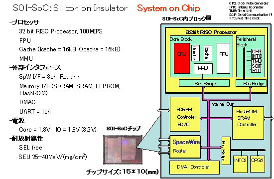
This developmental system has reached the stage of practical application. For example, Mitsubishi Heavy Industries has succeeded in commercializing an SoC with high radiation tolerance as the highest-performance logic IC. In this SoC, various components including a 32-bit microprocessor, memories, and space wire interfaces are integrated on a single chip, exhibiting extremely high performance. In addition, the SOI structure and ingenious circuit of this SoC enable the complete prevention of single-event latch-up and marked suppression of the soft error rate (radiation tolerance of 25-40 MeV/(mg/cm2), much higher than that of state-of-the-art consumer SOI devices, 1 MeV/(mg/cm2) or less). For the time being, this SoC is scheduled to be mounted on the next astronomy satellites. Mitsubishi Heavy Industries is planning to apply its SoC to equipment in other fields that have potential for the mass production of SoCs.
In this research, we successfully established a foundation to develop ultrahighly integrated ICs with high radiation tolerance at high flexibility and low cost by combining the ISAS's radiation hardening technologies and state-of-the-art domestic consumer SOI technologies and by adopting cell libraries with the prospect for consumer applications. This foundation enables the development of various logic ICs with high radiation tolerance, not limited to the SoC commercialized as described above, and is expected to serve as a key strategy in the Japanese space industry and technical fields that require high radiation tolerance.
Nineteen papers showing the results of basic research carried out to obtain this achievement are published in IEEE Transactions on Nuclear Science, the world’s most prestigious academic journal on the effects of radiation on semiconductor devices. These studies were twice given Conference Outstanding Paper Awards in the IEEE Nuclear and Space Radiation Effects Conference (NSREC) annually held in the US.
Research team:
Hirobumi Saito (Professor), Kazuyuki Hirose (Associate Professor), Daisuke Kobayashi (Assistant Professor)
ISAS, JAXA
Figure: SoC commercialized by Mitsubishi Heavy Industries (©Mitsubishi Heavy Industries).
|
|