Succeeded in Prototyping Integrated Circuits (ICs) with
a Small-Volume Production System (Minimal Fab)
- JAXA and AIST paving the pathway to
minimal fab-produced ICs aboard spacecraft -
May 10, 2019 (JST)
National Research & Development Agency
Japan Aerospace Exploration Agency (JAXA)
National Institute of Advanced Industrial Science and Technology (AIST)
Highlights
• Japan Aerospace eXploration Agency (JAXA) is aiming to produce integrated circuits (ICs) for space applications with a small-volume production system (Minimal Fab) (Figure 1). Using a practical SOI-CMOS with two-layer aluminum wiring process, Technology 2018, developed by National Institute of Advanced Industrial Science and Technology (AIST) (Figure 2), JAXA has designed an IC which contains around 1000 transistors (4bit shift resistor and an I/O circuit) and manufactured a prototype chip (Figure 3) whose operations has been demonstrated successfully (Figure 4).
• AIST has built a fully automatic Minimal Fab system, which enables a circuit designer to manufacture a semiconductor device on his own by operating a series of manufacturing equipment. Maneuvered by a JAXA circuit engineer, the new system has proven itself and produced the above ICs.
• These prototyping and operational demonstration have opened the way to manufacturing electronic devices aboard spacecraft with a Minimal Fab process, which is expected to broaden the applications of the new process.
Overview
JAXA and AIST have been conducting a joint research project concerning the applications of a small-volume production system (Minimal Fab) (Figure 1) to aerospace research and development applications, and have demonstrated for the first time in the world that the new system can realize ICs intended for use in space.
AIST has developed a fully Minimal Fab SOI-CMOS with two-layer aluminum wiring process, called “Technology 2018” (Figure 2). Since each piece of technical information and the whole operating procedure of the Technology 2018 process are computerized, the operation of the entire equipment is completely automated, requiring no special skills, which is the outstanding feature of Minimal Fab.
Capitalizing on expertise in designing and manufacturing ICs accumulated through many spacecraft development projects, JAXA has designed an IC which contains around 1000 transistors (4bit shift resister and an I/O circuit), prototyped using Technology 2018 (Figure 3), and demonstrated normal functionality of each circuit element (Figure 4).
The demonstration has proved the effectiveness of a Minimal Fab system, which can produce a wide variety of ICs for space applications in small batches in short periods. Efforts will be continued to put this technology into practice.AIST will accelerate its efforts in developing application of Minimal Fab not only to spacecraft but to many fields of industry including the production of IoT (Figure 5) devices, which is one of the purposes of this project.
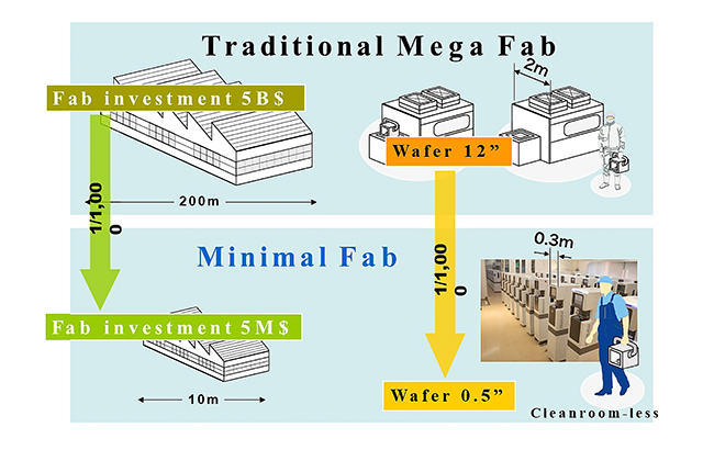
Fig. 1: Traditional Mega Fab and Minimal Fab
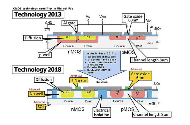
Fig. 2: Practical SOI‐CMOS Technology 2018 developed for Minimal Fab
© AIST
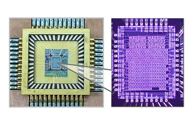
Fig. 3: The Photo of fabricated IC (right) and packaged chip (left)
© JAXA
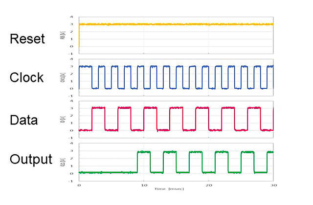
Fig. 4: Measured waveform of 4bit Shift Register
※ Input data is read out after 4 clock cycles, and function have been confirmed.
© JAXA